Germanium on silicon near infrared photodetectors
Overview
Introduction
Material growth and characterization
Device fabrication and characterization
Introduction
Objective
- realization of NIR photodetectors
for Optical communication at (1.3-1.55mm) integrated on silicon
Motivations
- optoelectronic integrated
circuits (OEIC) (compact, reliable, fast, new functionality)
- silicon based optoelectronics (VLSI compatibility– low
cost, high yield)
Problems
- lattice mismatch
- thermal coeff. mismatch
- height mismatch
- power supply compatibiliy
In the last decade, applied research in optoelectronics has
addressed long-haul high-performance point-to-point transmission in the near
infrared (NIR) at 1.3 and 1.55 microns, where silica optical fibers exhibit
minimum losses and limited dispersion. This well established technology, along
with the unprecedented demand for internet services, cable TV, video on demand,
e-commerce and so on, is promoting a broader acceptance of fiber optic
communications also in Wide and Local Area Networks (WAN, LAN), Metropolitan
Area Networks (MAN), fiber to the home (FTTH) connections and even to the
smaller distances characteristic of intrachip transmissions. In this framework,
it has become essential the development of a suitable technology in the form of
optoelectronic integrated circuits (OEIC). OEIC's, combining optical and
electronic devices and functions, compared to state-of-the-art board- or
card-assembled solutions, are expected to match the requirements for very high
performance while encompassing compactness and lightweight, reliability, low
parasitics, mass-producibility and low costs.
Monolithic integration is the most elegant solution because, embedding the
realization of optoelectronic and electronic devices in a single fabrication
process, it is expected to avoid most of the alignment and interconnection
problems, thus providing matchless yield and reliability.
Regardless the centrosymmetry and indirect bandgap of the electronic structure
of Si Ge and their alloys, it has been demonstrated that near infrared light can
be emitted, guided, switched and detected. Ge thin films on Si for NIR
photodetectors are the main subject of this presentation.
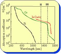
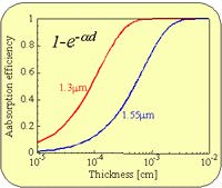
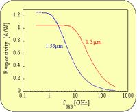
Responsivity is mainly related to the absorption efficiency 1-exp(a d). Large a and d ensure that most photons are captured. However, since a too much large a could reduce the speed of response due to transit time limitations, high absorption materials are preferred. Typically, coefficients a >104 cm-1 are needed in order to keep absorption lengths in the 1-4 mm range and allow a sufficiently wide bandwidth. If the photodiode is well designed, the bandwidth is limited by the transit time effect.

Growth
A successful heteroepitaxy (in terms of crystal quality) can be
accomplished if two materials have the same crystal structure and lattice
parameter. Silicon and Germanium have the same structure (diamond-like) but Ge
has an atomic spacing about 4% larger than Si. This large lattice mismatch
introduces strain, a crucial factor in the growth of SiGe epilayers on Silicon.
The first SiGe layers deposited on Si find energetically convenient to adjust
the lattice through a compression in the growth plane and a tensile strain along
the normal (strained layer), whereas the thick Si substrate remains
substantially undistorted. As the growth proceeds, the large accumulated strain
tends to let the Ge restore its own lattice spacing. This is referred to as
relaxation, and the epitaxial film becomes relaxed. Relaxation takes place once
the strain reaches a threshold level corresponding to a critical thickness hc,
and is always associated with the generation of a large amount of line defects
both in the growth plane (misfit dislocations) and perpendicularly (threading
dislocations). Due to the thickness required for high responsivity, the only way
to get thick pure Ge layer is to use relaxed layer and minimize the dislocation
density.
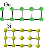
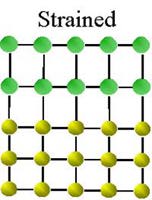
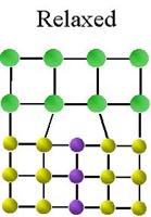
Strain relief through relaxation is always associated to the generation of a network of line defects lying in the growth plane (at the interface), called misfit dislocations. A misfit dislocation cannot terminate within the bulk, but must either end upon itself forming a closed loop or terminate intersecting another defect, or, more generally, stopping at the nearest free surface. An ideal picture, with defects entirely confined in the growth plane, requires the dislocations to sweep across the interface up to the end of the substrate. Dislocations can move, but their limited velocity (in terms of chip or substrate dimensions) and the proximity of other dislocations or the presence of pinning sites stop their propagation by bending them up. Defects that propagate across the epilayer are called threading dislocations. Hard to estimate, the density of threading dislocations is proportional to the lattice mismatch and, unless drastically reduced, is very detrimental for applications.
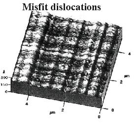
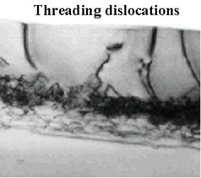
We have developed a new method for reducing dislocation density based on a two step growth followed by thermal annealing
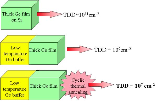
The idea of the low temperature (LT) Ge buffer layer comes from the need of a simple way to relax the large amount of strain in a very thin region close to the heterointerface, releasing the stress energy through the insertion of dislocations instead of islands formation. The thermally induced stress induces faster dislocation glide and annihilation, responsible of TD density reduction at an enhanced rate (as the glide velocity goes up TD’s travel more and the probability of annihilation increases).
Material characterization
Ge film have been characterized by transmission electron microscopy (TEM) and etch pit density count (EPD)

buffer without annealing TDD = 9.5·108 cm-2

buffer + annealing 780/900°C TDD = 2.7·107 cm-2
Effect of dislocations
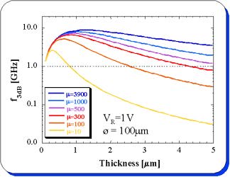
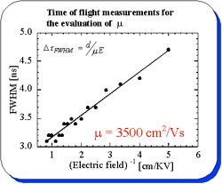
Dislocations affect crystal quality, in terms of carrier mobility for example. The figure shows how the device speed is limited as a function of the photodiode intrinsic layer thickness for different mobilities. Dark current is affected by high dislocation density as well. Since the main contribution comes from generation current in the space charge, dislocations, reducing carrier lifetime, increase the dark current. Threading dislocations are also reported to be sources of local breakdown which affects life and reliability of the devices.
The Ge film has been characterized by means of optoelectronic measurement of an interdigited geometry in order to evaluate the mobility-lifetime product and the carrier mobility.
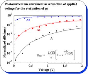

The carrier lifetime in sample A2, calculated from the measured mobility-lifetime product and the carrier mobility, is 850 ps. This is several orders of magnitude shorter than in electronic-grade bulk Ge, in the 10-3-10-6s range. This short lifetime can be related to recombination at threading dislocations still present in the epilayer.
Fabricated photodiodes
Metal-semiconductor-metal i-Ge/Si (1998): 
Heterojunction photodiodes i-Ge/Si (1999-2000)

p-i-n heterojunction n+-Ge/i-Ge/p+-Si (2000-2002)

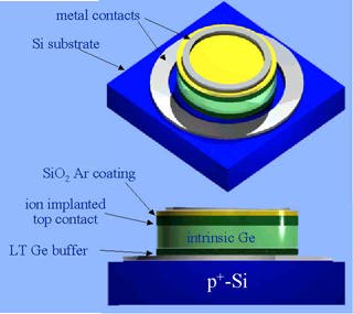
Device fabrication (p-i-n)
Steps:
- substrate cleaning
- low temp Ge buffer
- Ge epilayer
- cyclic thermal annealing
- ion implantation
- AR coating deposition
- fabrication of mesa
- contact deposition
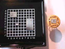
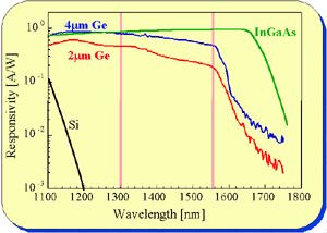
Device characterization: responsivity vs l
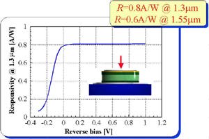
Device characterization: responsivity vs V
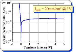
Device characterization: dark current
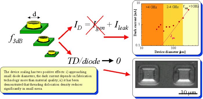
Comparison:

On the dark current:

Device characterization: speed
Time response of the 135mm-diameter device to the 120ps pulse
train from Nd:Yag laser emitting at 1.32mm
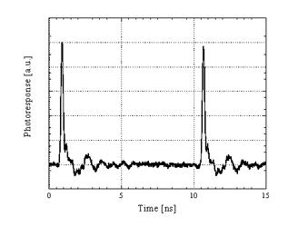
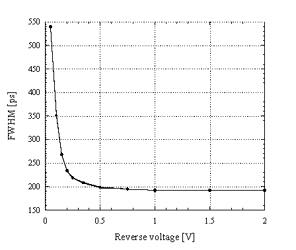
Results are consistent with an RC limited response, being the measured junction capacitance and the series resistance 0.7 pF and 250 W, respectively. Devices with larger areas exhibited proportionally slower responses; we can therefore infer that the response time is still dominated by the junction capacitance, leaving space for further improvements by mesa-diameter reductions. The latter statement is also supported by an estimate of transit time from mobility, which yields 50 ps at a reverse bias of 1 V. The measured speed of photoresponse corresponds to a frequency cutoff higher than 2.5 GHz, and therefore enables our photodetectors to operate according to OC-48 at bit-rates above 2.5 Gb/s.
